Packaging Lab
• Packaging of microelectronics circuit
• Tied closely with IC micro-fabrication process
• To build a packaged device using a wafer

Packaging Lab
• Packaging of microelectronics circuit
• Tied closely with IC micro-fabrication process
• To build a packaged device using a wafer

Packaging Lab
• Packaging of microelectronics circuit
• Tied closely with IC micro-fabrication process
• To build a packaged device using a wafer
WELCOME TO PACKAGING LAB
About Packaging Lab
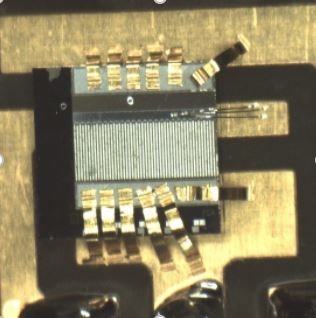
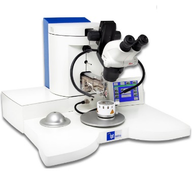
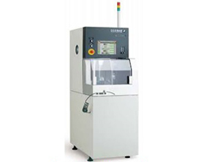
Packaging of microelectronics circuit is the science and art of establishing interconnections for MEMS and IC devices. MEMS is relatively a new field which is tied closely with IC micro-fabrication process. All packaging applications can be summed up in three terms: performance, reliability and cost.
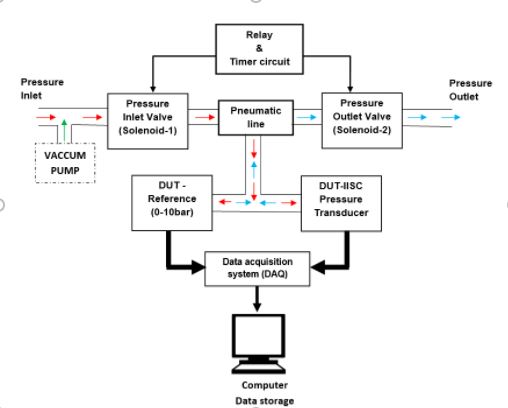
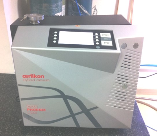
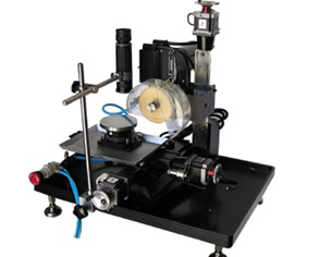
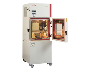
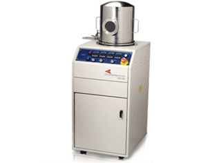
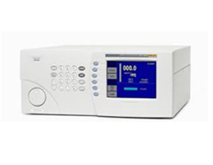
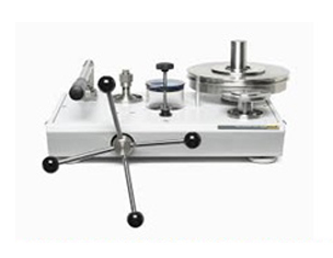
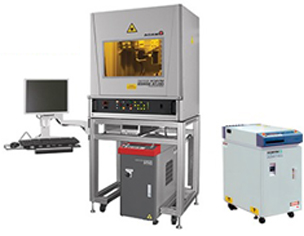
Packaging lab is located in the third floor of the CeNSE building #TF 32, is a 2000 sq feet air conditioning lab, housing Equipments/tools to enable packaging of various MEMS and IC devices. The lab has facilities for Wafer Dicing, Die Attach, Ball/Wedge bonding, Laser welding, Soldering, and High Magnification Microscope for assembly, packaging and testing of MEMS and IC devices. It also has facilities for Low/High pressure calibration, Acoustic calibration with data acquisition systems for performance studies and characterization of various transducers. As one of the supporting facilities at CeNSE, MEMS and IC Packaging lab provides all the facilities required to build a packaged device using a wafer